May 13, 2014
ISEM researchers turn the world of nanomaterials upside down
A new material the thickness of a single atom could pave the way for a range of new tiny electronic devices.
A range of new and more powerful tiny electronic devices could be possible following the development by University of Wollongong (UOW) researchers of an innovative new method of building two-dimensional materials the thickness of a single atom.
Nanomaterials, though only less than one-hundredth the thickness of a human hair, have large surface areas that enhance chemical reactivity, strength and electrical properties, which makes them ideal building blocks for tiny electronic devices that range from pollution sensors to wearable power generation and storage.
These tiny yet powerful materials are typically engineered in a lab from metals, ceramics, plastics or combinations of materials using one of two common methods.
The top-down approach involves removal or exfoliation of layers of atoms or a process that transfers a pre-designed shape onto a surface; while the bottom-up constructions uses sophisticated chemistry to build the material atom-by-atom.
The range of materials used in the bottom up method of constructing two-dimensional materials for electronic devices has limited their range of applications. Metal oxides have a much broader range of uses but they are difficult to build and tend to be weak when layered to form larger shapes.
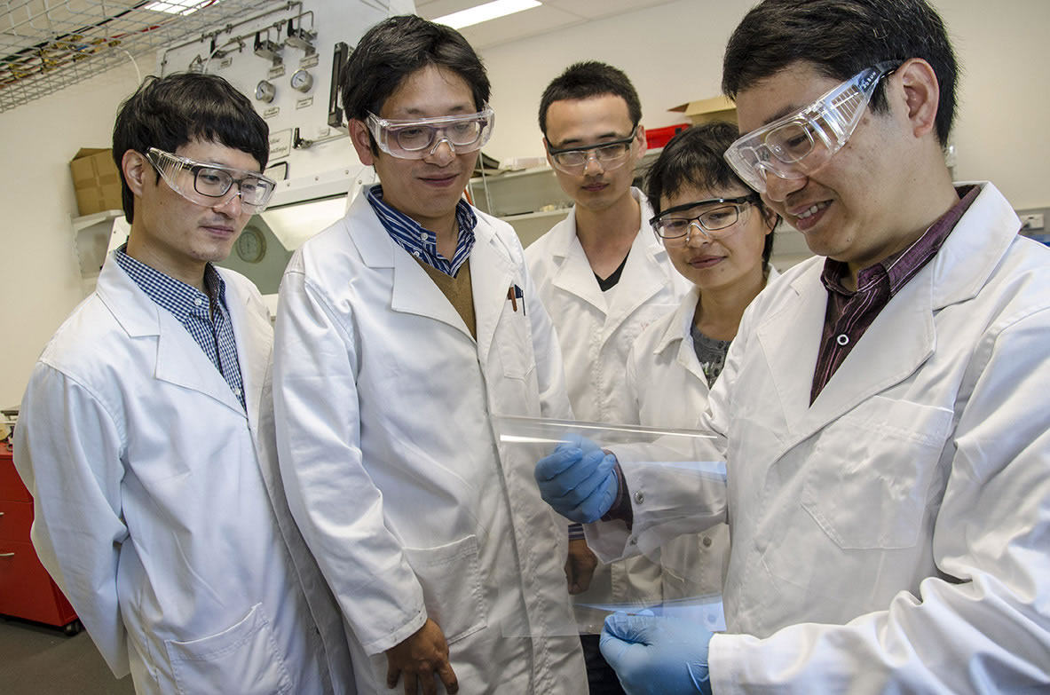
A research team led by Associate Professor Jung Ho Kim and Dr Ziqi Sun from the UOW-based Institute for Superconducting and Electronic Materials (ISEM) has overcome this problem and demonstrated an innovative way to fabricate ultra-thin two-dimensional layers of metal oxide materials.
The team’s method of using solvents to separate and re-assemble atoms offers a relatively simple yet controllable fabrication route for 2D structures. Combined with a single layer of the so-called wonder material, graphene, their 2D material was highly responsive to ultraviolet light and could be used as a transparent, wafer-thin light sensor.
Dr Ziqi Sun said the technology could have rewarding applications in energy generation and storage.
“Ultra-thin devices made with metals provide superior energy conversion and storage because they have a very large surface area within an atomic-scale size. The problem has been that a precisely controlled way of constructing these materials was unresolved.
“A simple method of assembling these materials as we have demonstrated is very promising for developing nano-sized electronics such as sensors and energy conversion and storage devices. The approach we have used could easily be adapted to other compositions of metals, which is important for enabling higher performance in the electronic devices of the future. We believe that this work opens many new possibilities for the field of materials science.”
The research paper ‘Generalized self-assembly of scalable two-dimensional transition metal oxide nanosheets’ was published in the journal Nature Communications on 12 May.
More: isem.uow.edu.au