
UOW research and innovation

Electron Microscopy Centre

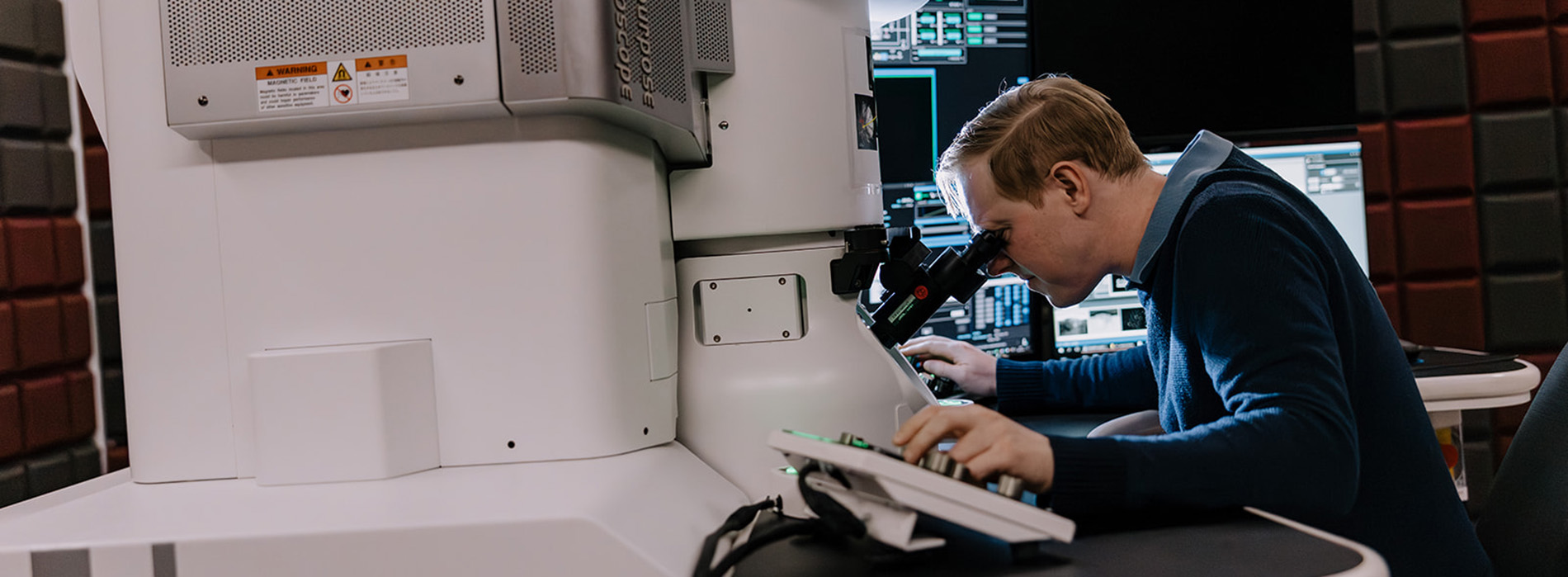
The UOW Electron Microscopy Centre (EMC) is a state-of-the-art research facility dedicated to providing high-quality electron, conventional, and cryogenic electron microscopy solutions. Featuring advanced microscopy suites and fully equipped sample preparation laboratories, the Electron Microscopy Centre offers a comprehensive range of instrumentation and techniques for material characterisation.

Equipment and services

With 11 high-end Microscopes, 6 multi-parameter Flow Cytometers (including one Cell Sorter) and Mass Photometry our facility enables research throughout the University of Wollongong and broader Illawarra region.

The facility is managed by two specialist staff who are available for instrument training, experimental development, application and technical support.

The EMC and its specialist staff provide quality microscopy solutions and training to students, commercial organisations, industry and government agencies. Our services include:

  • Microscope use and sample preparation
  • Consultancy services
  • Contract research and development projects
  • Collaborative research and development projects
  • Training and seminars

The EMC comprises a total of seven microscopy suites that optimise individual microscope performance, two modern and well-equipped specimen preparation laboratories, utility/service corridors plus open plan offices for research and technical staff, higher degree research (HDR) students and visiting academics.

Bookings

Book our facilities online

Conditions

The EMC provides its users with the materials characterisation results needed for their research projects. EMC staff work with users on a case-by-case basis to assess the scope, duration and technical complexity of the task at hand and tailor user access and training to suit the individual and/or research projects.

After completing the induction and registration process, users may contact individual staff members by email to arrange for training/access to the microscopes and their correlated ancillary sample preparation equipment.

Each new user/research project will be assessed by the staff member(s) responsible for particular microscopes and a decision will be made: (i) whether to train the new user for an independent user licence on a microscope and its correlated sample preparation equipment or, (ii) whether it is more time and cost effective for the work to be conducted by the EMC staff on the user's behalf. In this manner, through combinations of collaboration and assistance from EMC staff, users can make the most efficient use of their sample preparation and microscope beam -times and be assured of high quality research outputs.

New users will only be trained for an independent licence when they demonstrate a clear need for more than 8 hours of data collection on the JEOL JSM-6490LA or 16 hours of data collection on the JEOL JEM-F200, the JEOL JSM-7001F and the JEOL JSM-7500FA. Access to the JEOL JEM-ARM200F is currently fully supported by Dr Lachlan Smillie and Dr Qiang Zhu.

Acknowledge us

As part of the terms and conditions of use of the EMC, all users, supervisors and project leaders are requested to acknowledge the use of particular facilities in all their written communications and oral presentations.

User acknowledgement is an important metric by which the performance of the EMC is judged and it enables the EMC staff to continue supporting users and expanding the range of services and capabilities that can be provided.

Please include the following acknowledgement(s) in all outputs which involve the use of EMC facilities and staff.

The acknowledgement may take the following forms:

  • The authors acknowledge use of facilities within the UOW Electron Microscopy Centre.
  • The authors acknowledge use of the facilities and the assistance of (Name of EMC staff member/s) at the UOW Electron Microscopy Centre.
  • This research used equipment funded by the Australian Research Council (ARC) Linkage, Infrastructure, Equipment and Facilities (LIEF) grant (ARC-LEIF Grant number)  located at the UOW Electron Microscopy Centre.

ARC-LIEF Grant numbers for the specific microscopes:

  • JEOL JEM-ARM200F: LE120100104
  • JEOL JEM-2011: LE0237478
  • JEOL JSM-7001F: LE0882613
  • FEI NanoLab G3 CX: LE160100063

All supervisors/project leaders using EMC facilities and staff are requested to email a complete list of their publications to the staff member responsible for the instrument in question at the end of each calendar year.

Content to come.

Transmission electron microscopes

The JEOL JEM-ARM200F is a 200kV probe corrected scanning transmission electron microscope (STEM) capable of atomic resolution imaging. At 200 kV the microscope features a resolution of <0.08 nm, while at 80 kV a resolution of <0.14 nm.

The microscope features a large area SDD EDS detector that allows elemental mapping with atomic resolution. Moreover, the microscope is equipped with a Cold Field Emission Gun with a resolution of 0.3 eV, which coupled with the GIF Quantum imaging filter, enables not elemental analysis at the atomic level determination of electronic structure; i.e., oxidation state, chemical bonding, surface plasmons, etc.

  • HAADF, ABF, SE/BSE STEM detectors
  • HR pole piece with up to 35o tilt range.
  • Tomography insert with up to 70o tilt range.
  • JEOL Cold holder (Liquid nitrogen temperature).
  • JEOL Centurio SDD detector with 100 mm2 detection area (~1 sr).
  • Gatan UltraScan 1000XP CCD camera (2k x 2k).
  • Gatan Quantum 963 SE imaging filter.

The JEOL JEM-F200 is a cold FEG TEM/STEM capable of running at 200 or 80 kV. At 200 kV the microscope features a resolution of 0.23 nm in TEM mode and 0.16 nm in STEM mode. 

The microscope features two large area (1.7 Sr) EDS SDDs suitable for high throughput elemental mapping for elements above Li, and quantisation for elements above F. 

The microscope additionally features a Segmented Annular All Field Detector (SAAF) which is suitable for STEM imaging of, for example, magnetic domains. 

The microscope is also equipped with: 

  • Conventional STEM BF and ADF/HAADF detectors. 
  • A Gatan RIO CMOS TEM camera with 4k by 4k resolution capable of 20-160 FPS. 
  • An autoloader for compatible single and double tilt specimen holders. 
  • Heating, cooling and mechanical testing specimen holders can also be used with manual loading.
  • HR pole piece with up to 35o tilt range 
  • Tomography insert with up to 70o tilt range.

Scanning electron microscopes

The JEOL JSM-7001F is a 30 kV analytical thermal field emission gun scanning electron microscope capable of 3 nm spatial resolution. It is well suited for the detailed characterisation of conductive/coated samples. The large area EDS detector enables rapid quantitative microanalysis and elemental mapping while the high resolution EBSD system enables orientation mapping in scanning and transmission modes.

The JEOL JSM-7500FA is a 30 kV semi in-lens cold field emission gun scanning electron microscope capable of 1.4 nm spatial resolution. It is well suited for the characterisation of insulating and nanomaterials, medical and biological samples. The gentle beam irradiation technique provides exceptional image quality at acceleration voltages as low as 0.1kV. This reduces charging effects in uncoated insulating materials and beam damage in electron-sensitive materials. The transmitted electron detector can attain a resolution of 0.6nm at 30 kV and is suitable for imaging thin foils or nanosized materials on thin support films.

  • SE, BSE, transmission detectors
  • Up to 40 mm diameter, 500 gm samples on a 5-axis compu-centric sample stage

The JEOL JSM-6490LA is a 30 kV conventional tungsten filament, variable pressure scanning electron microscope. It is well suited for basic structural imaging of large (or component sized) engineering materials and wet, biological or cryogenic samples at a maximum resolution of 3.5 nm (at 30 kV). The large area EDS detector enables rapid quantitative microanalysis and elemental mapping while the cathodoluminescence spectrometer allows investigation of trace elements, electronic structure and stress in a range of non-metallic materials.

The FEI Helios NanoLab G3 CX is a state-of-the-art dual (electron and ion) beam analytical scanning electron microscope and highly targeted sectioning tool. Using the focused ion beam 3D analytical datasets of electron images and EDS/EBSD datasets can be generated though serial sectioning of a region of interest (up to ~50 um3) or to prepare targeted electron transparent lamella for high resolution TEM investigation or atom probe samples. 

  • SE, BSE and STEM detectors
  • Pt, C and N2 (charge neutralisation) gas injection
  • Samples must fit within a 25 mm radius and be less than 10 mm high for general samples
  • Oxford instruments X-maxN 150 mm2 123eV SDD energy dispersive X-ray detector
  • Oxford instruments NordlysMax 3 High speed EBSD camera
  • Integrated AZtec synergy software suite comprising AZtec HKL for EBSD and AZtec energy and AZtec ED and EBS4 for 3D dataset acquisition and analysis

PI-95 TEM Pico-Indenter

The Bruker PI 95 TEM Pico indenter enables researchers to probe the mechanical properties of nano-sized materials inside the transmission electron microscope. The holder is able to acquire quantitative nanoscale mechanical data in different modes including compression, tension, bending and scratching, while the high spatial resolution of the TEM allows for simultaneous observation and recording of the deformation phenomena, such as dislocation bursts, phase transformations, shear banding, etc. Licenced TEM users could be trained to use this holder. Standard TEM usage charges applied.


Gatan 652 In-situ Heating Holder

This holder takes standard 3mm disk-type TEM specimens. These can be either bulk foils or nanoparticles on support films (on grids). The holder has an operating temperature range up to 900 deg C routinely, and up to 1000 deg C for very short intervals. It features double tilting (+/- 25 degs), which permits crystallographic studies of such phenomena as phase transformations and recrystallization. It is compatible with both of the EMC’s JEOL TEMs. EDS analysis/mapping cannot be done during heating, due to infrared radiation blinding the detector. However, analysis after the holder has cooled back down to room temperature is possible, albeit with a small collection angle. Due to thermal drift, high resolution studies are not practical with this type of holder. However, imaging at up to several hundred thousand times is feasible. Access to this specialised holder is fully supported via EMC staff. Experiments should be very carefully planned as in-situ heating often leads to results which differ from bulk data, due to surface and thin specimen effects and oxidation inside the microscope. Detailed thermal properties (eg DTA/TGA) of the material to be studied MUST be provided beforehand, to identify the temperatures of interest and to avoid the risk of phases melting during heating, which can cause very costly damage both to the holder and to the microscope.  There is no additional charge for using this holder (aside from fully supported microscope usage costs). The holder uses sacrificial tantalum washers to prevent specimens sticking to the holder. In the event that the specimen sticks to the washers, the user will be charged for replacement costs at $50 per pair.


In-situ testing stage for FEGSEM

The Micomecha SAS 3 kN deformation stage works within the JEOL 7001F FEG-SEM for in-situ imaging/EDS/EBSD/EDS+EBSD work or on a benchtop as a sub-size sample mechanical property tester. Its capabilities are as follows:
- Room temperature tension, compression, 3 point bend, bi-axial tension and shear
- The ability to heat standard size dog-bone samples to 600 °C along with the ability to semi-quench them through the passage of a liquid inside the SEM chamber.
-  A cooling module capable of cooling down to liquid nitrogen temperature.
The use of this stage is fully supported by EMC staff. Special usage charges covering both microscope time and stage are applied: for the first 6 hrs within the 24hr period - $210, each subsequent hour is $10. No subscription discount is available.


Thermo Scientific™ μHeater holder

The μHeater is a high-vacuum compatible, ultra-fast heating holder for in-situ investigations of small samples (i.e. lamella, nanoparticles) up to 1200°C. The μHeater uses small MEMS based chips (consumables) as a heater, which rapidly heat a sample at a rate of 0.01 to 104 °C/s with temperature settling to within 1 °C. The μHeater is fully integrated in the Helios NanoLab CX G3 dual beam instrument. All standard analytical channels including EBSD, EDS and SIMS are available during all experiments.

The μHeater has an additional four contacts that can be used for biasing experiments up to ±40V and/or for sample resistance measurement.

The use of this holder is fully supported by EMC staff.


Optical microscopes

  • Edwards TIC vacuum pumping station and desiccator for SEM and TEM samples
  • JEOL EC-52000IC ion cleaner for TEM holders/samples
  • JEOL EM-21090 cryogenic holder and EM-SHU2 control unit for TEM at -160°C
  • JEOL JEC-4000DS dry pumping station for TEM holders
  • Kammerath & Weiss GmbH 3 kN tension/compression stage with resistance heating up to 900°C
  • Leica EM KMR3 Glass knifemaker
  • Struers Emco-Test DuraScan-70 Vickers hardness tester (10 gm to 10 kg)
  • XEI Scientific Evactron-25 decontaminator/plasma cleaner for TEM holders and SEM and TEM samples

Contact us


Contact the UOW Research Infrastructure team to connect with the right facilities and experts and achieve your goals.